Thursday, December 31, 2015

New Year's EVE & EVITA

Last Post of 2015.

Tonight, a bit later, I will be celebrating the New Year, but for the next few hours I am working hard on a new 50x50 pcb design - more on this later.

This week, as readers might know,  I have been involved in a Trans-Atlantic collaboration to develop a new prototype board for an Embedded Video Engine or EVE chip - manufactured by Glaswegian firm FTDI.

In a hectic week, a team working in the UK and also in Northern California - have got the hardware running - and are now able to produce a big bright graphics display on a large screen monitor - using virtually any "Arduino -like" microcontroller development board.  For only a few dollars - you can now add high quality 24 bit video and audio to your latest project - and there is not a Rapberry Pi in sight.

Here's an example of what James and Felix (pictured) achieved in California on Tuesday.
Felix solders whilst James writes code...
Meanwhile in the UK I was successfully creating an image of a big red blob....


The EVE chip is normally used to produce a video interface for LCD touchscreens - but with a bit of tweaking and a few precision value resistors we have got it producing reasonable quality 24-bit RGB video for displaying on monitors or TVs that have the usual VGA (15way Sub D) connector.

This allows virtually any small microcontroller to produce good quality graphics - and in the case of the prototype - any board that supports the Arduino expansion headers.

With a few clever tweaks to the timing, James in California has succeeded in obtaining a 1024 x 768 60Hz resolution - sometimes known as XGA.  This exceeds the published specification of the chip, only by a small margin - but as James is expert on these matters, he assures me that there is no cause for concern.

Just in Time for the Party - Meet EVITA

Whilst the prototype was a quick design just to prove things are working - and so far they have exceeded all expectations, I am currently working on an upgraded  new board, that is most likely to be a commercial product.


The EVITA board uses the same FT812 EVE chip, but adds a microSD card socket, audio output from a 3.5mm jack and unlike the prototype is now 5V tolerant - so you will be able to use this on a 5V Arduino - without "Fear of Frying".  EVITA offers a better overall layout, more signals are available for the experimenter, and better still, it is compatible with GameDuino 2.

If you add EVITA to a humble Arduino, you have essentially the basis of a full computer system, with connectors for Keyboard, Mouse, Audio and glorious XGA video output.

Right from the start, EVITA is open source hardware and open soft software.  If you are good at fine, surface mount soldering, you could purchase a bare board cheaply, stock up on the components and build your own in a couple of hours. All of the information is available online, including datasheets, code libraries and a vibrant community forum.

In the next few weeks there will be some more pcbs released in the 50x50 format. These will allow you to add a custom ARM processor to EVITA and make up exciting new projects.

More of this in 2016


Ken


Tuesday, December 29, 2015

Making a new product in a month - An Engineers Life in 140 Characters or Less

A new product always starts with an idea.

In late November, I had been reading about various ways of producing a low cost VGA video output from a microcontroller.  Having dabbled with VGA on the ZPUino soft core processor on the Papilio Duo from Gadget Factory, I realised that if any small microcontroller could be assisted to produce stunning video effects and support a sophisticated user interface at minimal cost - then it would be a major innovative step.

I read about the new EVE (Embedded Video Engine) ICs from FTDI in Glasgow and ordered a dev-kit in early December. At the same time I started work on a board layout for a new minimalist VGA shield.

1st Draught - Will it all Fit?
I had been musing throughout the Autumn about a new board format of just 50mm x 50mm  - in order to make full use of the special offers from the low cost Chinese board houses - so my first attempt was to see if I could even get the VGA and PS/2 connectors onto the standard board template. Above is my efforts - dated November 26th.

Over the 1st weekend of December (5th, 6th) my ideas blossomed, and grew - and so by the end of the the first week of December I had a 56 pin QFN package footprint worked out plus something that approximated to a FTDI EVE chip on a board. With the basics in place - it was just a case of finishing the layout and tidying up.

Main FT812 IC partly routed

By the 9th of December - the design was nearly ready for sending off - and this was further reinforced by a message from my board-house saying that pcb designs sent in before the midnight on the 10th of December would be delivered before Christmas - and with a 10% discount.

Almost ready for prototype production
On December the 10th - a very busy day to get 2 new designs delivered to @Ragworm by midnight. This tweet hints at the urgency that Thursday

So the pcbs went off to Ragworm on the night of 10th December, and then we were in for a bit of a wait, until they were delivered before Christmas. Also on the evening of the 10th, I forwarded the EagleCAD files to my friend James Bowman (@GameDuino) who lives near San Francisco - so that he could have a go at having a duplicate set of pcbs made - independently of mine.

In the mean time I got on with another pcb design - this time for a low energy Bluetooth device - and spent 3 wonderful days up in North Wales at #BothyHack3 - where I designed some, yet more pcbs.

On the 22nd of December, I received a package containing the prototype boards - I tried a bare board for size on one of the FPGA platforms we were considering:


So that evening I built up the first prototype:


Christmas activities then got in the way for a few days - but on the 24th James reported that his pcbs had just been delivered in California from China - having been held up for over 24 hours in Fremont, California:


So with Christmas almost upon us - Festivities kind of impeded progress - also known as a well deserved rest. I have done 20 unique board designs in the last 24 months......

So on the Morning of 28th December, I crawled out of the post Christmas hangover haze and thought about exercising the new VGA hardware.  It took longer than I thought - but by 1am, and a couple of false starts - the VGA hardware sprung into life and created its first image.


From large red blobs served in the early hours of the morning I progressed to a simple text display:


But then on Tuesday evening - James came back with the stunning tweet that he had pushed the resolution up to 1024 x 768  60Hz. So at that point I suggested that I get my coat.....


A few hours later, James was coding furiously and Felix was soldering - the picture from California says it all - all produced by the FT812 EVE chip - and James' custom Forth processor:


With only a couple of days remaining of 2015, I barricaded myself in the back bedroom - and bashed out an greatly improved pcb layout - all ready for manufacturing next week when the world wakes up from its Festive Haze:

                                               Introducing - on New Year's EVE  - EVITA


I hope you have enjoyed this light-hearted look at how modern engineers collaborate across global frontiers and timezones - using social media to full advantage - in order to expediate the development of a new fun product.  From concept to first prototype executing code and exceeding all expectations in just a month.  Shouldn't we all be working smarter, not harder?

And remember - when it's 2am in Britain - it's only "Beer o'clock" in Northern California!

Thanks to all my friends and colleagues in Kent, Sussex, Denver and Northern California who have helped make this happen so quickly.

Now off to the Monson Road Social Club- for some New Years festivities and the odd beer or three.


Happy New Year - and all the best for 2016!


Colour Coding - Part V

In this post I will take you though the process of getting the FT812 SVGA shield up and running.

But first a little success story..........

SVGA Shield generates a big red blob!

Building the SVGA shield hardware was fairly quick - but what I didn't anticipate was a 16 hour day with a couple of false starts before I got it to produce it's first image.
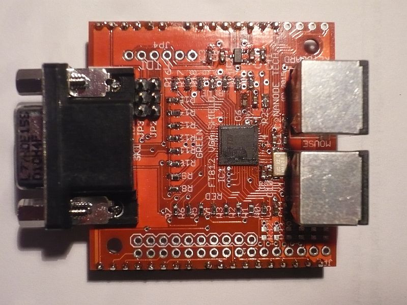
Hardware

It's always the case when you produce a new board design - that feeling of concern whether you have actually managed to get all the tracks right and everything connected correctly.

In the case of a break out board - this risk is minimised - because you have access to every pin on the IC - in theory.  However, in this case, because of the tight tracking around the QFN package, I had omitted to bring out some of the unused tracks - those involved with the clocking and latching of data to the non-present LCD. It was a gamble - but fortunately it paid off.

What I hadn't anticipated was the difficulty of soldering down the QFN package. Whilst it might look soldered - there is the chance that not all the pads have correctly wicked the solder under the package - and there were indeed, about half a dozen pads which required some remedial work.

A tip for the future is to use slightly longer pads for the QFN.  This ensures that there is perhaps 0.5mm of pad extending beyond the package - and it makes it so much easier to run additional flux and solder underneath the package with a manual soldering iron.

Unfortunately one of the non-soldered pads was VCCIO2 - which is a VCC power supply pin that supplies power to approximately half the chip - including all the RGB outputs, the Hsync and the Vsync.  This meant that a lot of time was wasted trying to fight unfamiliar firmware wondering why half the IC wasn't working.

Apart from the unsoldered pads, which were eventually traced and re-soldered, the layout of the pcb is essentially correct - so I have faith that I now have a "working wireless".

Firmware

The firmware is based on the example supplied by FTDI for their Application Note AN 312.

This is intended to work with the STM32F407 Discovery Board - and as I already have several of these, it is quite a good place to start.

The firmware is based on their generic FT8xx hardware abstraction layer - which covers all the ICs in the FT8xx and FT81x range.  A header file FT800.h contains all the register names - but these memory mapped  registers are different for the FT80x and FT81x - so you have to make sure you select the correct set. It took me quite a while to establish exactly what set I needed, and to deselect the ones I didn't.

Once this was done, the chip started to show signs of life, and the 12MHz external crystal oscillator sprang into life.  The firmware reads back the chip ID - and if it doesn't see "7C" returned over the SPI bus - it knows that there is a fault, and halts.  I chose this to light up a red LED - so I knew that when the red LED went out - all was correctly set up.

Video Timing

The FT812  is a very versatile IC and can produce screen resolutions of up to 800x600 pixels, however, it needs a bit of setting up so that it's video output is something that a multi-sync monitor can actually sync to.

After quite some considerable experimentation with different sync timings and pixel clock frequencies I found that I could generate 800x600  56Hz with sufficient accuracy that the monitor would accept it. Some of the video standards use a positive going sync pulse - and the timing registers for this had to be carefully adjusted to get the right duration and timing.

The parameters I finally arrived at are as follows:

   //  SVGA // 800 x 600 56Hz VGA display parameters
  lcdWidth   = 800; // Active width of LCD display
  lcdHeight  = 600;        // Active height of LCD display
  lcdHcycle  = 952;       // Total number of clocks per line
  lcdHoffset = 96; // Start of active line
  lcdHsync0  = 0; // Start of horizontal sync pulse
  lcdHsync1  = 890; // End of horizontal sync pulse

  lcdVcycle  = 625; // Total number of lines per screen
  lcdVoffset = 2; // Start of active screen
  lcdVsync0  = 0; // Start of vertical sync pulse
  lcdVsync1  = 623; // End of vertical sync pulse
  lcdPclk    = 2; // Pixel Clock
  lcdSwizzle = 0; // Define RGB output pins
  lcdPclkpol = 1; // Define active edge of PCLK

These were used with the external 12MHz crystal oscillator, and the sync timings are approximate - and could possibly be better tuned.

Next Steps

The FTDI test code has allowed me to get the board up and running and produce my first video output. The code was relatively easy to understand - if not somewhat verbose, plus the fact that it catered for about 6 different ICs across several platforms - so was a little more complicated than it need have been.

The next step is to incorporate the GameDuino2  code Library - written for Arduino platforms etc - which will allow a somewhat higher level access to the video effects that the FT812 is capable of. This will be the subject of the next post.

It should be possible to port the GD2 library to mbed - and this would give immediate access to a very wide range of microcontrollers - including NXP, Freescale, Nordic etc.  It will also allow the SVGA shield to be used on the STM32F Nucleo boards,  Discovery F7 and the Maple Clones (STM32F103).

During testing, I also made good use of an old ATmega328 board I designed a few years back - the WiNode.  It's an uncluttered Arduino "clone"  that works at 3V3. I use these for quite a few small projects - as I have about 50 remaining in stock from an earlier project. They are in the form of a through hole kit - and can easily be soldered up in about half an hour.

The WiNode pcb can provide just the basics - a minimal 3V3 Arduino with access to the headers. This board will execute the GameDuino2 Library - with minimal modifications - and has the benefit of  a uSDcard holder on the underside of the board. There is also a battery backed RTC, 32Kx8 SRAM and an H-bridge that can be used as a class D digital amplifier for driving small speakers.  Adding video to such a useful board with further increase its application.


WiNode and SVGA Shield together for comparison
Conclusions

The SVGA shield concept works and is capable of producing an 800x600 SVGA video output for a monitor - using an IC that was really intended for compact LCD modules.

The hardware was simple and straightforward - the biggest problem was reliably soldering all the pads of the 56 pin QFN package.

The board can also accept a PS2 keyboard and mouse - and a welcome addition on a future version would be a microSDcard socket - allowing images to be down loaded from card.

The board works with a very basic 3.3V  SPI interface up to 30MHz  spi-clock - requiring just 5 signals - plus 3V3 and 0V.  It can be added to any microcontroller that presents the original Arduino expansion header pattern, with the SPI bus available on D11,D12, D13.

Some hours later - I could do this.....


Tuesday, December 22, 2015

Colour Coding - Part IV

The new FT812 VGA Shield  - with PS/2 Keyboard and Mouse Inputs

A couple of weeks ago, I completed the pcb layout for the universal VGA shield - a small 50mm x 50 mm pcb that fits a range of popular 3.3V microcontroller development boards. Any dev board that supports the basic Arduino style headers can use this board - and that opens it out to a very wide range of boards.

The board provides
  • A powerful 800 x 600 graphics co-processor   - the FT812 from FTDI
  • PS/2 Keyboard connector
  • PS/2 Mouse connector
  • Additional UART via FTDI cable
The freshly minted pcbs arrived in today's post - just in time for some development work over the Christmas holiday period.

The boards may be fitted to several popular microcontroller and FPGA dvelopment boards  - including

  • STM32F  Nucleo boards
The VGA shield fits neatly on any STM32F Nucleo Board
  • STM32F7 Discovery Board
Fitted to the underside of a STM32F746 Discovery board
  • Gadget Factory  Papilio Duo FPGA Board with Xilinx Spartan 6 FPGA

Fitted to a Papilio Duo FPGA board
  • Any board that supports Arduino headers with 3V3 signalling!
My 3V3 ATmega328 "WiNode" pcb - which also has a SDcard
The FTDI FT812 is a complete graphics co-processor - intended for driving colour LCDs. With a little bit of tinkering, we can make it produce a VGA signal - suitable for displaying on any flatscreen monitor.  The PS/2 keyboard and mouse interfaces offer the extra connectivity to bring a full user interface to your latest microcontroller project.

The FT812 embedded video engine removes the burden of producing a colour graphical interface from the microcontroller - and allows quite stunning GUIs to be produced from even a basic 8 bit microcontroller.

The FT812 is accessed over a SPI bus - and for convenience this has been brought out to the standard Arduino headers.  Provided that your dev-board works at 3V3 - then this board should be compatible.

Instead of using an 8-bit microcontroller, such as the ATmega328 - this board has been produced with much faster, 32-bit processors in mind.  These include the STM32Fxxx range of ARM Cortex M3, M4 and M7 processors from ST Microelectronics, and the Soft Core processors available from the Gadget Factory Papilio Duo FPGA board.

Some Hardware Details.

The FT812 is accessed via the SPI bus  - on the usual D11,D12,D13 Arduino pins. Additionally there is a Chip Select on D9 and an optional INT on A1, and a Power Down PD on A2.  PD acts as a reset an normally needs to be pulled high. 

The FT812 has 8-bit outputs for the Red, Green  and Blue components of the video signal. These digital outputs are recombined in a resistor network to produce an analogue component video signal of approximately 0.7V amplitude.

The value of the resistors are chosen to be as close as possible to increasing powers of two - starting at 499 ohms.  There is a useful blog post and a XL spreadsheet describing how the resistor values are chosen for a similar VGA project here.  It should be noted from the XL spreadsheet that the most significant resistor (499 ohms) appears to give a step discontinuity in the output - this may be minimised (on paper) by lowering this value to approximately 470 ohms. This has yet to be tried in practice.

The values finally chosen for the resistor network are:

R7      499R    (470R)
R6      1K
R5      2K
R4      4K02
R3      8K06
R2      16K
R1      31.6K
R0      63.4K

The shield also provides a PS/2 Keyboard and Mouse interface.

For full hardware details - please refer to Colour Coding Part III

As this shield is merely a prototype, it has not configured to allow the audio output of the FT812 IC. A second iteration of the PCB will include a 3.5mm jack socket for sound output and a microSD connector for local image storage.

Firmware Development

Fortunately FTDI have provided a comprehensive set of code examples for the FT81x. These include header files describing all the internal registers, and walk you through the process of configuring the main registers for various display setups.

I will use these as the basis of the initial C code so that I can bring the IC up - using known, tried and tested code.

To maximise the usefulness of the VGA board - and make development simpler and more accessible to all, I have decided to write the code using the mbed compiler, and use a STM32F103 Nucleo board - as the development platform. 

The reasons for this is that the mbed online toolchain is free to use and has good library support, the code will be portable across a range of different target platforms - including the STM32F7 Discovery board - and the Nucleo boards are really cheap.

This avoids the whole situation of having to deal with codesize limited Keil or IAR toolchains, and added complexity of the STM32xxx HAL shenanigans!  

It also make the code portable across a wide range of mbed supported platforms - from IC vendors including Freescale, NXP, Nordic, Renesas, Maxim, Wiznet and ST. In fact any vendors platform that supports the Arduino style headers - at 3V3! can be used.

Meanwhile, in sunny Northern California, James Bowman of GameDuino - has recreated the VGA board and is writing some drivers so that it can be run from his J1b Forth processor - a softcore cpu - hosted on the Gadget Factory Papilio Duo, - which is a Xilinx Spartan 6 FPGA board.  

This little VGA shield will also allow VGA graphics for any softcore processor - such as recreated 6502, Z80 etc.  The FT812 takes all the grunt of graphics generation away from the cpu - so even a little 8 bit processor - recreated in a FPGA from a 40 year old design can have graphical output that was never an option back then.

Other FPGA boards such as the Arty - a $99 Artix board from Xilinx can also be fitted with this VGA/Keyboard/Mouse  (VKM) shield - in fact anything that has the all important Arduino headers! 

There will be a full report in a later post as we get the firmware up running - both in mbed C and J1b Forth on this new unit.


Monday, December 14, 2015

So Many Ways to Skin a Cat......


SIMPL code can do this to an otherwise blank screen
Background

I have recently been experimenting with the J1b Forth processor,  running on a Papilio Duo board - a low cost FPGA development board from Gadget Factory.

The J1b has a cycle time of 12.5nS and can conduct an empty Forth DO LOOP in just 100nS. This is seriously quick  - an major asset for such a simple processor.

The only problem I have, is that the J1b is programmed in Forth, on top of it's own assembly language - and neither of these really appeal for quick experimentation.  

Forth is a tremendously powerful language - but you have to practice hard to keep your brain up to speed with it - so this is why I am a proponent of a novel cut down version of Forth - essentially a minimal Forth-Like interpreted language, which I call SIMPL.

From Arduino to ZPUino - and everything between

As I find coding in Forth a bit hard on the brain - I have got interested in other minimal interactive languages - which are ideal for testing out new hardware.

SIMPL was inspired by Ward Cunningham's Txtzyme Interpreter - from 2013 - which is written in C and programmable into various dev boards like Arduino and Teensy.

Txtzyme is a very small text interpreter, where single characters are interpreted as function calls. These are used to invoke the various "hardware helper" functions - that are part of Arduino - such as digitalWrite, analogRead, millis, delay etc.  

Txtzyme only has 13 functions in it's basic form - but the beauty of it is that it forms a minimum framework which is easily extended. Also because it has been written in C (all be it Arduino dialect) it is easily ported to virtually any other microcontroller. The core of Txtzyme uses only about 1300 bytes of program space on an ATmega328.

Txtzyme is a minimalist interpreter, which allows immediate and interactive control of the hardware - from a few serial commands. Txtzyme is Forth-like in it's behaviour, and uses a stack to process commands.

In the last 2 years I have added extra functionality to it, and tried it out on a number of resource limited processors - from the Arduino to custom soft-cores - such as the ZPUino - which runs on the Papilio Duo dev board.

I have added integer maths, and the ability to handle 32 bit numbers.

In the Spring of 2013, I extended Txtzye to allow new user subroutines to be defined, and a means to store these user routines in RAM.  I called the resulting program SIMPL - which is an acronym for Serial Interpreted Minimal Programming Language.

SIMPL has been developed specifically to make interaction with new processor hardware both fun and easy.

Commands take the form of a lowercase letter - usually preceded by a number. Unlike Forth whitespace is rarely used at all - and the space character has a special function of pushing a second numerical parameter onto the stack  - to give two operands for arithmetic etc.

Here are some of the basic commands

d   Allocate a digital pin for input or output
h   Set the allocated port pin high
l    Set the allocated port pin low
m  A millisecond delay
p   print out the value on the top of the stack
u   A microsecond delay
s   Sample the analogue input pin
t   Print out a time stamp in microseconds - useful for timing operations
{   Start a loop of instructions
}   End a loop of instructions
_   Text Identifier for print out   eg. _Hello World_

Then we have arithmetic and logical operators

+  Add the top 2 items on the stack
-   Subtract
*   Multiply
/   Divide

&  Bitwise AND
|   Bitwise OR
~  Invert
^  Bitwise XOR

To light a LED on Digital 13:    13dh     

13d just allocates an output pin  - in this case Digital 13

To flash a LED 10 times:   13d10{h100ml500m}

h is the comand to set the allocated pin high, and l to set it low.

100m is a 100mS delay.

Extending the Language

SIMPL can be extended with "colon definitions"  These start with a colon : and are given a capital letter as their function name - so only 26 new definitions are permitted

For Example, to acknowledge a command by printing ok:   

:O_ok_  

Any text included between the _ _ is printed to the terminal.

So concatenating these commands 

13d10{h100ml500m}O    - flash an LED, on digital 13, 10 times and acknowledge with ok when finished

The size of this program is just 18 bytes plus a carriage return. That makes it small enough to be send as a packet over a wireless link.

You can then give this function another name - like "F" - for flash-LED

:F13d10{h100ml500m}O

Timing

SIMPL has the native ability to be able to time-stamp your code.  For example, if you wanted to generate a million cycles of square wave via an output port:

t1000000{hl}tO

t effectively prints out the microsecond count at the time it is called - so the above example provides a start time and an end time for a million cycle output

The response from this command sequence is 

13569162
17507533

OK

So subtracting the numbers - we can calculate that 1 million output pin toggle cycles was executed in 3.938371 seconds - so a frequency of  253.9kHz. This is approximate because it includes the printout time (11520 characters per second) and the overhead of setting up the loop.

With these few short examples - we can see that SIMPL is very extensible.

Graphics

SIMPL is easily extended to allow any coded function to be called from the terminal. 

I programmed in the ZPUino soft core onto the Papilio Duo, with a modified a version of SIMPL -so that I could take full advantage of the Adafruit GFX library - and output graphics to an 800 x 600 pixel VGA screen.

I have included a SIMPL primitive "g" which wll plot a single pixel at y,x. 

Primitive "a" sets the 16 bit colour value.

To plot a Line we define a new word L   :L 800{kg}   This draws a line 800 pixels long

To fill a field - we define a word F   :F600{kL} which draws 600 consecutive lines  - thus filling the screen

(in each case, k is the decrementing loop variable).

So to combine these into a repetitive screen clear routing  we define a new word S

:SaF   -   clear the screen with colour, a

Finally we set this up in a loop that cycles through all the possible values of a

65535S

At about 5 seconds for a screen wipe - this could take a few hours  (91 hours!)


Saturday, December 12, 2015

The Powers That Be.....

Recently I have been looking at performance of different computing machines over the decades, and how in the 70 years of British Computing History we have seen speed of operation increase, transistor count increase and cost decrease by several orders of magnitude.

Mathematician, and UCL lecturer Dr. Hannah Fry, recently hosted an excellent radio series on BBC Radio 4  "Computing Britain"  - a 10 part series available as a podcast  - as well as individual episodes. 

It was the first episode "Electronic Brains"  that triggered me into taking a closer look at some of the early British machines.

The first computers built in the 5 years immediately after World War 2 used thermionic valve (vacuum tube) technology, and consumed killowatts of power.   Studying these machines, specifically EDSAC - revolutionary in the late 1940s had a 512 word memory, and in terms of performance - about 600 instructions per second was all that could be achieved, and this was mostly down to the fact that the ALU handled data in a serial fashion - as you really cannot build a parallel 35 bit ALU with just 1500 triode valves - the 1940's switch equivalent of the transistor.

Jumping forward 25 years to 1965 and the PDP8 - this was the first of the mass-market "mini-computers". By this time digital hardware was transistorised - using DTL (diode, transistor logic) - essentially diodes were used to create the "OR" function, and a transistor was use for the invert or "NOT" function - thus allowing the full range of logic gate functions to be synthesised.

The first PDP 8 used about 1500 transistors (PNP germanium) and about 3000 diodes. The engineers at DEC worked hard to get the transistor count down - because back then a transistor cost about $2 or $3 each - but falling rapidly - and Gordon Moore's law clearly illustrates this point graphically.

The PDP8 used magnetic core memory - as was common at that time, and it was the memory cycle time of 1.5uS that had the most influence on the overall processing speed - allowing a typical 2 cycle memory reference instruction (Fetch, Execute) to run at 0.33 MIPS. Manufacturing core memory was very labour intensive - so the whole 4K word machine sold in 1965 for $18,000 - at a time when a new convertible VW Beetle cost $1750.

Ten years later, when the 6502 was created, the transistor price had fallen by 2 orders of magnitude per decade, and the whole CPU could be integrated on the one silicon die - allowing the 3510 transistor 6502 to be sold for about $20. Smaller integrated transistors meant faster operation - and so the 6502 could be clocked at 2MHz - allowing 1 million operations per second.

Another decade - now 1985, and the engineers at Acorn Computers were working on the first ARM processor. Here a tiny British design team, took a radical approach, that flew in the face of conventional cpu design wisdom, and created a 32bit RISC processor with just 25,000 transistors. The ARM1 ran at 8MHz and delivered a performance of 4MIPS.

It's contemporary - the Intel 80386 used 275,000 - more than 10X the transistor count.
The ARM 1, first ran April 1985 - and here I believe was the start of a revolution in computing devices. Intel continued to plug away at their '86 architecture - with it's transistor count and power consumption rapidly spiraling skywards.

By 1995 an Intel Pentium Pro used 5,500,000 transistors and a 307mm2 die whilst the ARM 700 still used a tenth of this number on a much smaller die area. The bigger the die area, the more likely that there is a defect, and this lowers the overall yield from the wafer. Hence the price per die increases.
Intel's insistance of sticking to a 1976 architecture has cost them dearly, both in terms of complexity, transistor count and cost. This is why ARM processors now dominate the mobile computing market, plus other low cost consumer and automotive markets.

Intel hit a brick wall around 2000, with their power greedy Pentium 4. I had a laptop at the time with a 3.06GHz P4 - which cooked your legs when using it on your lap. It took Intel a further 8 years to manoeuvre out of the P4 road block, and come out with their lower power Atom devices.
There has to be a way to reduce complexity - As Jean Claude Wippler stated:

"Four decades later, on a 2015-era 4-core 2.8 GHz i7 CPU with its advanced pipelining and branch prediction, each of the cores can process billions of instructions per second – with an optimising gforth compiler for example, the “1000000000 0 do loop” takes around 2 seconds – that’s 2 nanoseconds per loop iteration"

Well, as you know, the J1 Forth computer implemented as an open soft core on a $10 FPGA can also achieve credible results - executing the same billion empty loop "1000000000 0 DO LOOP " on an 80MHz J1b executes in almost exactly 100 seconds. About 100nS per loop - not bad for a device running 1 core and at 1/35th of the clock speed and a tiny fraction of the power.

If the J1 could run at 2.8GHz it would do the task in 2.85 seconds - only 2/3rds of the performance of the billion transistor Intel - What are they doing with all those other transistors........?

Here we see that a transistor count of 1 billion is not the best way to get a task done.

I am looking forward to exciting times ahead.......

Friday, December 11, 2015

Colour Coding - Part III

This is the first of my 5050 boards -
 that has gone to meet it's makers....

As Frankie Howerd used to say....

The Prologue

In the last week, I have designed a compact VGA generation pcb - which will provide a test bed for FTDI's latest second generation embedded video engine IC   ("Eve") -either FT812 or FT813  .

This board is in the form of a 50mm x 50mm shield - that will work with Arduino compatible devices - provided that they have a 3.3V system voltage (NOT 5V!!). The EVE IC  is not 5V tolerant!

This includes all STM Nucleo boards, STM32F7 Discovery board - and my own design "Piano Forte" board which is STM32F1xx, STM32F3xx or STM32F4xx with Arduino Headers.

The board also includes an interface for a PS/2 Keyboard and Mouse.

I have ordered a small batch of these boards from Ragworm - a UK PCB vendor, and hope to make some progress over the Christmas break.

Some Details

The VGA board uses a FT812 to generate the VGA signals in 24-bit colour at a resolution of 800 x 600 pixels.

The FT812 or "Eve" chip  (embedded video engine) is a very capable graphics co-processor with a 1MB frame buffer.  It can provide a low resource microcontroller with all the elements of a graphical user interface for just a few dollars.

The FT812 is connected to the host processor "Arduino" using a very conventional SPI interface, along with an interrupt line (optional) and a Power Down signal.

The FT812 provides 8 digital outputs for each of the RGB colours and each of these are weighted and summed together using a very simple resistor network  - to produce an analogue video signal of red green and blue components.

Whilst the board is arranged with Arduino style headers - it can be used with any other 3V3 dev - board - using jumper leads - as only 8 connections are needed to interface to it.

As this board is purely a VGA testbed - none of the LCD specific signals are brought to connectors.

The PCB supports a serial connection using an FTDI cable, plus a variety of different break-out options.

A set of optional resistors fitted to the underside of the PCB - allow it to be used solely as a passive VGA adaptor (without the FT812 fitted) - to work with the STM32F7 Discovery board - allowing up to 1024 x 768 7 bit colour.

The Hardware Set Up.

When used as a VGA generation shield for a 3V3  Arduino - like device - the following pins are used to access the FT812


D3  Keyboard Clock
D4  Keyboard Data
D6  Mouse Clock
D7  Mouse Data
D9  SPI CS
D11 SPI_MOSI
D12 SPI MISO
D13 SPI SCK

A1  /INT
A2  PD

Power is supplied to the board via the 5V power pin - and is regulated down to 3V3 by IC2 - a maximum of 300mA available from the MCP1702 regulator

An FTDI serial cable can be fitted into connector JP4 (next to the analogue inputs connector) and using a pair of jumpers JP2 and JP3  allows access to the D0 and D1 Rx and Tx pins.


Other Connectors

The remaining un-jumpered pins of JP5 provide breakout for the GPIO pins plus PD and /INT of the FT812. The additional pins - on the end of the Arduino "power" header give access to the resistive touchscreen sensing network - and could be used as such, or used carefully as 10 bit resistive analogue inputs.  


The backlight pin provides a 7-bit duty cycle PWM signal - of frequency between 250Hz and 10Khz.

Pixel Clock, Data Enable and Disp have not been routed out on the first prototype boards.
The Audio pin has not been routed out on the first prototype boards.

This board hopefully will provide the VGA graphics, keyboard and mouse interface to a variety of dev - boards, thus expanding their capabilities, manifold.  If the basics of the board are sound, it can be later augmented to cater for audio and a microSD card.

Introducing Eve.

The EVE chip has an impressive specification - here's a copy of the 1st page of the datasheet

The FT81x is a series of easy to use graphic controllers targeted at embedded applications to generate high-quality Human Machine Interfaces (HMIs).

 It has the following features:

  •  Advanced Embedded Video Engine(EVE) with high resolution graphics and video playback
  •  FT81x functionality includes graphic control, audio control, and touch control interface
  •  Pinout backward compatible with FT800 (FT810) and FT801 (FT811).
  •  Support multiple widgets for simplified design implementation
  •  Built-in graphics operations allow users with little expertise to create high-quality displays
  •  Support 4-wire resistive touch screen (FT810/FT812) 
  •  Support capacitive touch screen with up to 5 touches detection (FT811/FT813)
  •  Hardware engine can recognize touch tags and track touch movement. Provides notification for up to 255 touch tags.
  •  Enhanced sketch processing
  •  Programmable interrupt controller provides interrupts to host MCU
  •  Built-in 12MHz crystal oscillator with PLL providing programmable system clock up to 60MHz
  •  Clock switch command for internal or external clock source. External 12MHz crystal or clock input can be used for higher accuracy.
  •  Video RGB parallel output; configurable to support PCLK up to 60MHz and R/G/B output of 1 to 8 bits
  •  Programmable timing to adjust HSYNC and VSYNC timing, enabling interface to numerous displays
  •  Support for LCD display with resolution up to SVGA (800x600) and formats with data enable (DE) mode or VSYNC/HSYNC mode 
  • Support landscape and portrait orientations 
  • Display enable control output to LCD panel
  • Integrated 1MByte graphics RAM, no frame buffer RAM required
  • Support playback of motion-JPEG encoded AVI videos
  • Mono audio channel output with PWM output
  • Built-in sound synthesizer
  • Audio wave playback for mono 8-bit linear PCM, 4- bit ADPCM and ยต-Law coding format at sampling frequencies from 8kHz to 48kHz. Built-in digital filter reduces the system design complexity of external filtering
  • PWM output for display backlight dimming control 
  • Advanced object oriented architecture enables low cost MPU/MCU as system host using SPI interfaces
  • Support SPI data lines in single, dual or quad mode; SPI clock up to 30MHz 
  • Power mode control allows the chip to be put in power down, sleep and standby states 
  • Supports I/O voltage from 1.8V to 3.3V
  • Internal voltage regulator supplies 1.2V to the digital core 
  • Build-in Power-on-reset circuit  -40°C to 85°C extended operating temperature range 
  •  Available in a compact Pb-free, VQFN-48 and VQFN- 56 package, RoHS compliant


PCB - Second Function  - As a Passive VGA network for the Discovery F7 

The shield may also be used to fit to a STM32F7 Discovery board - which also has Arduino style connectors. The STM32F746 has an on-chip video generation engine, which synthesises the signals needed to run a colour LCD. Conveniently several of these higher bit colour signals and H-sync appear on the Arduino headers. 

When used in this mode - the following pins can be configured to have RGB data on them.

D0        Green 6
D1        H-Sync
D2        Red 7 
D5        Green 5
D8        Green 7 
D10      Red 6
D14      Blue 7
D15      Blue 6

VSYNC is missing but can be synthesised from H_SYNC used to clock a Timer input

To utilise this mode of operation it is necessary to fit the resistor network to the underside of the pcb and fit the jumper headers JP1 and JP5.  Ten jumper links are needed to connect every pin on JP1 across to its neighbour on JP5.

If using a F7 Discovery board, there is an additional SPI port and UART available - as alternative function on the Analogue Input Pins. The UART can be jumper selected using JP3 and JP4 so that it is accessible from the FTDI connector.  All of these pins accept analogue inputs of 12 bits

A0   PA0      UART4_TX
A1   PF10
A2   PF9     SPI5_MOSI
A3   PF8     SPI5_MISO
A4   PF7     SPI5_SCK        UART7_TX
A5   PF6     SPI5_NSS        UART7_RX


Applications

Colour graphics really makes computers come alive - and a simple video interface is an asset to any microcontroller.

It has been seen that the Gameduino and Gameduino2 provide a spectacular graphical environment for even the 8-bit ATmega328 Arduino.

Having a colour text output, that can be displayed on a large screen monitor - independent of an IDE- will give a whole set of new dimensions to developing and debugging code on any microcontroller.


The addition of a keyboard and mouse all makes for a better computing environment.

.